Apr 1, 2024
The hearts of the Super Nintendo
When I start studying a vintage system, the first thing I like to do is understand how its components work together at the hardware level[1].
Every computer has at least one heart which dictates the tempo to all the other chips. The CloCK output pin is connected to a copper line which spreads to most components, into their CLK input pin.
If you are mostly a software person like me, you may have never noticed it but all kinds of processors have a CLK input pin. From CPUs (Motorola 68000[2], Intel Pentium[3], MOS 6502[4]), to custom graphic chips (Midway's DMA2[5], Capcom CPS-A[6]/CPS-B[7], Sega's Genesis VDP[8]) to audio chips (Yamaha 2151[9], OKI msm6295[10]), they all have one.
How is the CLK generated?
The CLK can be generated by two types of components. One is a crystal oscillator which usually looks like a flattened capsule. The others are named ceramic resonators. These are vertical capacitor which look less high-tech than the crystals (and they also happen to drift over time).
An oscillator A resonator
Let's open it already!
With this in mind, let's peek inside a Super Nintendo. Can you find the CLK generators on a SNES motherboard? Clue: There are two.
Source. Click the image to find the CLK generators.
Two hearts
In the X2 slot, the blue thingy is a 24.576 MHz ceramic resonator. It is located on the side where the audio chips are so it sets the pace of the Audio Processing Unit.
In the X1 slot, the yellow one is labeled D21L3 . It is a 21.300 MHz oscillator. It is located near (and sets the pace of) the CPU and the Picture Processing Unit.
Documentation discrepancies
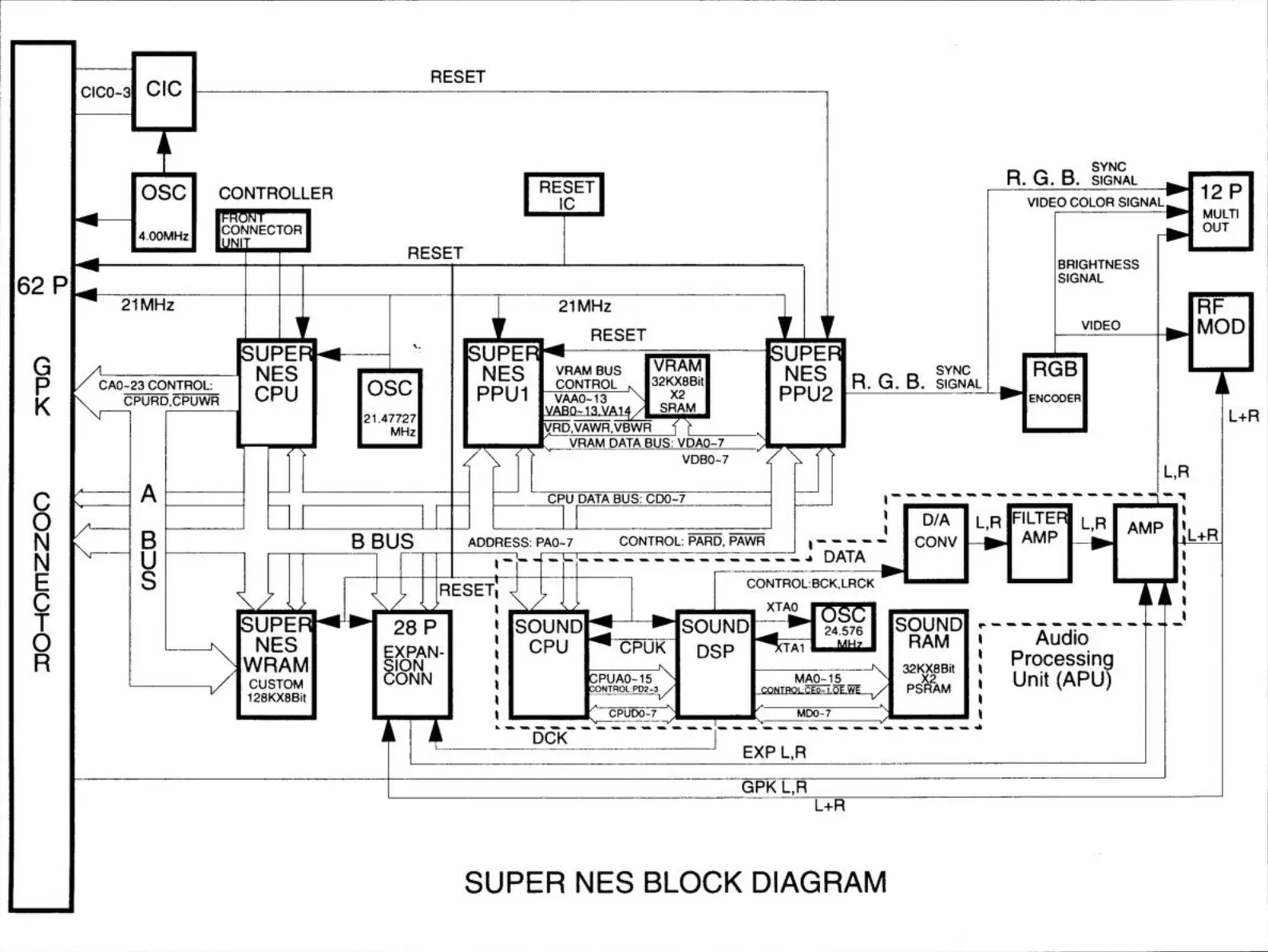
Looking at the Super Nintendo developer guide[11] reveals it does not match our observations.
The diagram shows not two but three oscillators (there is one feeding the CIC chip, responsible for copy-protection). We are missing one!
Moreover, the frequency for the CPU/PPU is documented as 21.47727 MHz but we found a 21.300 Mhz oscillator (this is a PAL motherboard, an NTSC one would have featured a 21.500 Mhz oscillator).
What is going on here?
CPU/PPU: From 21.500 MHz to 21.47727 MHz
If we look at the motherboard again, we will notice a red component in the lower left, just next to the oscillator. This red thingy is a variable capacitor (some people also call it a trimmer capacitor) which turns the 21.500 MHz frequency into 21.47727 MHz.
Why did the designers make it adjustable? The likely answer is that Nintendo feared the oscillator would deteriorate over time, and technicians would be able to tune it. They may not have been wrong since a common issue for the Super Nintendo console is to render in black and white. The solution is often to adjust the capacitor (or replace the oscillator)[12].
Dividers
There are only two "master" clocks in the console but none of the processors use them. What happens is that these masters go into dividers to create new clocks. The Ricoh 5A22 CPU for example, runs at 1/6 of the master clock, which results in 3.579545 MHz. Luckily, the SNES community (and nocash in particular) has documented all these dividers[13].
NTSC Timings NTSC crystal 21.4772700 MHz (X1) NTSC color clock 3.57954500MHz ( 21.4772700 MHz/6) (generated by PPU2 chip) NTSC master clock 21.4772700MHz ( 21.4772700 MHz/1) (without multiplier/divider) NTSC dot clock 5.36931750MHz ( 21.4772700 MHz/4) (generated by PPU chip) NTSC cpu clock 3.57954500MHz ( 21.4772700 MHz/6) (without waitstates) NTSC cpu clock 2.68465875MHz ( 21.4772700 MHz/8) (short waitstates) NTSC cpu clock 1.78977250MHz ( 21.4772700 MHz/12) (joypad waitstates) NTSC frame rate 60.09880627Hz ( 21.4772700 MHz/(262*1364-4/2)) APU Timings APU oscillator 24.576 MHz (X2) DSP sample rate 32000Hz ( 24.576 MHz/24/32) SPC700 cpu clock 1.024MHz ( 24.576 MHz/24) SPC700 timer 0+1 8000Hz ( 24.576 MHz/24/128) SPC700 timer 2 64000Hz ( 24.576 MHz/24/16) CIC clock 3.072MHz ( 24.576 MHz/8) Expansion Port 8.192MHz ( 24.576 MHz/3)
In total there are fifteen clocks in the Super Nintendo. Hopefully this solves the mystery of the "missing" oscillator from the documentation.
Enhancement chips
The SYS-CLK (21.47727MHz) line is fed into the cartridge port. This signal is normally not needed by the components in the cartridge. These are made of ROM containing the game instructions and assets which don't need a clock signal. So why route it there?
The answer is that it allows cartridges to embed processors of their own, called enhancement chips[14]. The most famous of these games is StarFox which features a "mario" SuperFX processor. The MARIO version has an internal divider which halves the clock to 10.738635 MHz. Later, GSU-1, versions ran at the full 21.47727 MHz clock.
Starfox PCB (source snescentral).
There is a second CLK line fed into the cartridge. It is CIC-CLK (3.072MHz) which is fed in the CIC chip located in the cartridge[15].
However SYS-CLK (21.47727MHz) was not always suitable. Some games, like Megaman X2 used a CX4 enhancement chip for graphic effects. If we open a MM2 PCB, we find a 20 MHz oscillator (X1 slot) which feeds the CX4 CLK pin.
Megaman X2 PCB. Notice the 20Mhz oscillator (source snescentral).
References
*