Inverse design and nanofabrication
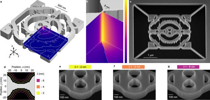
We use carefully measured fabrication constraints as input to size- and tolerance-constrained topology optimization17,18 aiming to maximize the projected local density of optical states1 (LDOS) at the geometric center of the domain, which is forced to be solid. The procedure for measuring the fabrication constraints is detailed in Supplementary Section 2. This ensures that the optimization is protected from local lightning-rod effects at the surface and instead achieves robust confinement inside the dielectric bowtie24. Our devices are based on 240 nm crystalline (100) silicon membranes (n = 3.48) suspended in air, patterned with electron-beam lithography, dry etching, and selective vapor-phase hydrofluoric acid etching. We optimize a cyclic dry-etching process36 to minimize the critical dimension while tolerating periodic sidewall roughness in the form of scallops37, see Methods. We note that surface roughness and the size of the scallops could be reduced by hard etching masks. The fabrication constraints are quantified as a set of critical dimensions, which we define through minimum attainable radii. For our process, we find the radius of curvature of any solid feature, r s ≥ 10 nm, and any void feature, r v ≥ 22 nm. The critical radii are limited by proximity effects during electron-beam lithography but it is possible to go below these limits with manual shape modifications of the exposure mask, see Supplementary Section 3. From systematic tests we find that it is possible to obtain a mean bowtie bridge width of 8 nm in a localized area, which we include as a third critical radius of curvature, r c ≥ 4 nm, at the center of the design domain. The topology optimization targets a maximum LDOS around λ = 1550 nm by tailoring the material layout in a small square domain with 2λ side length. We fabricate DBCs based on these parameters and the resulting structures show excellent agreement with the designed geometry as displayed in Fig. 1c. The high fidelity of the fabricated structures compared to the design demonstrates explicitly the value of directly including the measured fabrication constraints in the topology optimization.
The quasi-normal mode of the structure (including the tethers used to suspend the cavity, cf. Fig. 1c) is calculated using a finite-element method and we project the electric field ∣E∣ on the symmetry planes of the structure in Fig. 1a, b. We calculate the effective mode volume38
$$\frac{1}{V}={{{{{{{\rm{Re}}}}}}}}\,\left[\frac{{\epsilon }_{r}({{{{{{{{\bf{r}}}}}}}}}_{0}){{{{{{{\bf{E}}}}}}}}({{{{{{{{\bf{r}}}}}}}}}_{0})\cdot {{{{{{{\bf{E}}}}}}}}({{{{{{{{\bf{r}}}}}}}}}_{0})}{\int _{V}{\epsilon }_{r}({{{{{{{\bf{r}}}}}}}}){{{{{{{\bf{E}}}}}}}}({{{{{{{\bf{r}}}}}}}})\cdot {{{{{{{\bf{E}}}}}}}}({{{{{{{\bf{r}}}}}}}})\,dV+i\frac{c\sqrt{{\epsilon }_{r}}}{2\omega }\int _{S}{{{{{{{\bf{E}}}}}}}}({{{{{{{\bf{r}}}}}}}})\cdot {{{{{{{\bf{E}}}}}}}}({{{{{{{\bf{r}}}}}}}})\,dA} \right],$$ (1)
with E(r) and ϵ r (r) the electric field and dielectric constant at position r, respectively. ω is the complex angular eigenfrequency of the cavity mode and c is the speed of light. The mode volume is in general a function of position, but for this to be a robust and useful definition, we evaluate it at the center of the cavity, r 0 . We find V ~ 0.08(λ/(2n))3 and Q ~ 1100, around λ = 1551 nm. The volume integral is over the entire simulation domain, while the surface integral should be evaluated on the outer boundaries and in practical calculations only constitutes a minor correction38 for cavities with Q ≫ 10, such as our DBCs.
We stress that the bowtie, along with all other details, are emergent features arising entirely from the inverse design process. Similarly, the fact that the mode volume falls deep below the diffraction limit of V = (λ/(2n))3 is a result of our algorithm aiming to optimize the LDOS in a limited domain. Gondarenko et al.15 used inverse design to obtain the first DBC with confinement in air, and concluded that the bowtie shape reduces V as well as that the ring gratings increases Q. While these features can be identified qualitatively from our inversely designed cavities, the performance of intuition-based cavity designs is inferior to topology-optimized structures17. Although the very large parameter space for the inverse-design algorithm makes it impossible to ascertain if the resulting design is a global optimum, it is interesting to note that the angle of the bowties are ~90°, that the bridge width equals 2r c , and that the voids surrounding the bridge are rounded with ~r v . These are exactly the parameters that were recently established as the global optimum for confinement of light inside bowties24 and the minor deviations reflect the fact that our algorithm optimizes LDOS, i.e., it targets not only the smallest V but, at the same time, the largest Q for the given footprint and our fabrication constraints.
Although we unambiguously demonstrate photon confinement deep below the diffraction limit, the modes are so compact that we cannot measure the precise size of the mode39. Therefore, measuring the width of the fabricated silicon bridge is crucial for rigorously comparing theory and experiment for DBCs. However, the bridge width of a few nanometers is close to the resolution limit of conventional microscopy methods, such as scanning electron microscopy. We therefore fabricate three sets of DBCs, each of which subject to a global geometry-tuning, δ, of the entire mask, thereby shrinking the exposed areas (air) in incremental steps of 2 nm as shown in Fig. 1d. In order to further validate the yield and reproducibility, we fabricate and characterize six nominally identical copies of each geometry-tuned device. Representative SEM images of each of the three geometry-tuned devices are shown in Fig. 1e–g and the 2 nm systematic variations are clearly observed in the change of the fabricated bowtie dimensions. We measure a mean bowtie bridge width of 8 nm, 10 nm, and 16 nm, for the three geometry-tuned devices, respectively. See Methods and Supplementary Section 4 for further details on the SEM characterization, and Supplementary Section 6 for an overview of devices characterized in this work.
Far- and near-field measurements
We characterize the devices using confocal cross-polarized microscopy (see Methods) and a representative reflection spectrum is shown in Fig. 2a. This spectrum shows the cavity mode as a feature around 1520 nm. The DBC mode interferes with the low-Q vertical cavity mode formed by the (~3 μm) air gap between the silicon device layer and the silicon substrate. This results in a Fano resonance, which is well known from confocal characterization of nanocavities40. The Fano line shape takes the form
$$F(\omega )={A}_{0}(\omega )+{F}_{0}\,\frac{{\left[q+2(\omega -{\omega }_{0})/{{\Gamma }}\right]}^{2}}{1+{\left[2(\omega -{\omega }_{0})/{{\Gamma }}\right]}^{2}},$$ (2)
where ω is the frequency, ω 0 is the DBC resonant frequency, Γ is the linewidth, A 0 (ω) is a linear function representing the background low-Q mode, q measures the relative amplitudes between the main and the background modes, and F 0 is a constant scaling-factor. The spectra for all six copies of each of the three geometry-tuned devices shown in Fig. 1e to g are displayed in Fig. 2b–d. We fit the Fano model locally around each resonance and extract ω 0 and the quality factor Q = ω 0 /Γ for all 18 devices of the three global geometry-tuning parameters. Figure 2e shows the mean and standard deviation of the resonant wavelength, λ 0 , and Q, for each δ. We obtain a mean spectral shift Δλ = (40.4 ± 0.6) nm between each incremental value of δ = − 2 nm from a linear fit and find that the standard deviation of the resonance shift of each set of geometry-tuned devices is ≤ (4 ± 0.6) nm. That is, the six nominally identical copies has spectral shifts ≤ Δλ/10, which corresponds to the devices being identical within ∣δ∣ ≤ 0.2 nm.
Fig. 2: Optical far-field characterization of dielectric bowtie cavities. a Broadband spectrum of a cavity with δ = − 6 nm. The cavity mode interferes with a background mode yielding a Fano resonance centered at λ ~ 1520 nm, highlighted by the red box. b–d Spectra for six nominally identical devices for each tuning δ = { − 2, − 4, − 6} nm. The spectrum of each copy is offset incrementally by 0.25 nW nm−1 for clarity. The full spectrum for cavity 5 is shown in a. The red lines show fits to the Fano lineshape. e Mean and standard deviation of resonant wavelength λ 0 (blue, left) and quality factor Q (red, right) against δ, extracted from the fits in b–d. Full size image
While far-field measurements give important insights into the spectral properties of DBCs, they do not allow extracting information about the mode shape and confinement. We therefore interrogate the near-field immediately above the DBCs using a scattering-type scanning near-field optical microscopy (s-SNOM), where a continuous-wave laser is focused on an oscillating atomic force microscope (AFM) silicon tip scanning across the DBC. Figure 3a shows the measured topography, which provides a clear image of the device but also shows that the tip penetrates into the void features, implying that the measured geometry is convolved with the function describing the tip. For the near-field optical characterization we use a pseudo-heterodyne interferometric detection scheme, which strongly suppresses interference with the far-field background41. This experiment allows recording the optical spectrum of the cavity mode without exciting the low-Q background resonance. Figure 3b shows the measured amplitude at an effective height of 5 nm above the surface at the center of the DBC. We model the measured cavity mode using a Green-tensor formalism treating the tip as a polarizable sphere and find that the measured amplitude is modulated by the intensity of the cavity mode42. From a Lorentzian fit in the frequency domain we obtain λ 0 = (1489.4 ± 0.1) nm and Q = 370 ± 40. The reduction in Q arises since the s-SNOM tip acts as an additional loss channel for the cavity so the s-SNOM experiment measures a loaded Q. The deviation from a Lorentzian lineshape may be due to nonlinear interactions or coupling with the near-field tip43.
Fig. 3: Scattering-type scanning near-field optical microscopy (s-SNOM) of cavity mode. a Topography measured by atomic force microscopy (AFM). b Spectrum measured of amplitude of scattered field with Lorentzian fit, λ 0 = (1489.4 ± 0.1) nm and Q = 370 ± 40. c s-SNOM signal on resonance demonstrating strong field localization with excellent suppression of background noise. The white dotted box highlights a square domain with its side length given by the diffraction limit, λ 0 /(2n Si ) ~ 200 nm. The strong signal in the cavity voids arises due to complex interactions between the AFM probe and the cavity mode. d Normalized measured amplitude of the light scattered from the cavity surface with the voids blacked out. e Numerical simulation of experiment, \(f\)(σ = 37 nm) ∗∣E c ∣2, confirming photon localization below the instrument response function as explained in the main text. The s-SNOM measurements presented here were performed on cavity copy 3 (δ = − 4 nm), which has a mean bowtie width of 10 nm. Full size image