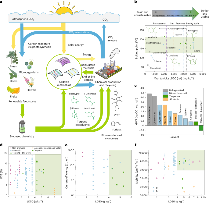
Materials and ink formulation
Indium tin oxide (ITO) coated glass substrates were purchased from Xin Yan Technology HK. Menthone (Men) and ethyl phenyl sulfide (EPS) were purchased from Alfa Aeser. Eucalyptol (Eu), limonene (Lim), pinene (Pin) and all other solvents were purchased from Sigma–Aldrich and used as received. For the PAL, PM6 and BTP-eC9 (1-Material) were mixed in a (1:1.2) donor to acceptor ratio at a 10 mg ml−1 concentration and dissolved in 1 ml of each of the ink formulations Eu:Tet (52:48), Pin:EPS (55:45), Lim:Ind (58:42), Men:Tet (55:45). For the hole transport layer, PEDOT:PSS (Clevios AL4083) was sonicated for 10 minutes and filtered through a 1.2 μm PTFE filter before usage. For the electron transport layer, PDINO was dissolved in methanol at a 1.5 mg ml−1 concentration. For the ZnO sol-gel ink, we mixed zinc acetate dehydrate with ethanolamine (21 µl) and 2-methoxyethanol solution (1 ml).
Solar cell fabrication
The ITO coated glass substrates were cleaned in detergent, deionized water, acetone and IPA by sonication, followed by oxygen plasma treatment to remove organic residues. Conventional architecture devices had an ITO/PEDOT:PSS (30 nm)/PM6:BTP-eC9 (120 nm)/PDINO (5 nm)/Ag (100 nm) stack and were fabricated as follows. First the PEDOT:PSS solution was spin coated at 4,000 r.p.m. for 30 s and annealed at 160 °C for 10 minutes. The PAL was deposited in air through blade coating at different speeds ranging from 5 mm s−1 to 50 mm s−1 and temperatures ranging from 20 °C to 90 °C; the optimized parameters are listed in Supplementary Table 4. Then, the PDINO solution was spin coated at 3,000 r.p.m. for 30 seconds in a nitrogen atmosphere, followed by thermal evaporation of 100 nm of silver through a shadow mask. Inverted architecture devices (single cells and modules) had an (ITO/ZnO(25 nm)/PM6:BTP-eC9 (120 nm)/MoO 3 (10 nm)/Ag(100 nm)) stack and were fabricated as follows. First, the ZnO sol-gel solution was spin coated at 4,000 r.p.m. for 30 s and annealed at 200 °C for 10 minutes to achieve a layer thickness of 40 nm. Then, the PAL (120 nm) was blade coated as described above. Then, lastly, 10 nm of MoO 3 and 100 nm of silver were deposited at specific areas through a shadow mask through thermal evaporation. All devices had an area of 0.1 cm2, except where specified. Large-area devices were defined following the same procedure and utilizing an evaporation mask with predefined areas (0.1–2.4 cm2). Modules were fabricated by patterning the ITO layer with a Yb-fibre laser (P1 Line), utilizing a scribing guide to remove material to allow for series connection (P2 Line) and a custom evaporation mask (P3 Line).
OLED fabrication
Super-green and Super Yellow materials were dissolved overnight at 85 °C in Eu at 2.5 mg ml−1. The ITO coated glass substrates were cleaned as described above. The conventional architecture devices were fabricated as follows. First, the Al 4083 PEDOT:PSS solution was spin coated at 4,000 r.p.m. for 30 s and annealed at 160 °C for 10 minutes. The PAL was deposited in air through blade coating at an optimized speed of 20 mm s−1, followed by thermal evaporation of 10 nm of Ca and 100 nm of Al.
OFET fabrication
Devices were fabricated in a bottom-contact top-gate configuration by evaporating 50 nm of gold on a glass substrate through a shadow mask to define source and drain contacts; channel lengths ranged from 30 μm to 100 μm. This was followed by solution deposition of the OSC film. CYTOP CTL-809M was spin coated at 2,500 r.p.m. and dried at 90 °C for 20 minutes, yielding a dielectric layer of 1 μm. Lastly, a 40 nm Al contact was deposited by thermal evaporation. O-IDTBR films were blade coated from a 2.5 mg ml−1 solution in Eu at 30 mm s−1 and 90 °C bed temperature to achieve 50 nm thickness. 2PyDPP-2CNTVT films were blade coated from a 2 mg ml−1 solution in Eu at 10 mm s−1 and 90 °C to achieve a 20 nm thickness.
Photovoltaic characterization
The current density–voltage (JV) curves were obtained by simulating the solar spectrum at AM 1.5 illumination through a 21 LED engine (Wavelabs Sinus-70) in a N 2 environment and using a voltage sweep from −1 V to 1 V in 0.02 V intervals while measuring the resulting current with a Keithley 2400 source meter. The instrument was calibrated with a certified 91,150 V silicon reference cell from Newport. The light intensity versus open circuit voltage (V oc ) and short circuit current (J sc ) measurements were carried out with neutral density optical filters (Thorlabs) ranging from optical density (OD) 0.1 to 4. The transmitted light can be calculated through the formula T = 10−OD, where T is a value between 0 and 1.
EQE
The EQE curves were obtained using a 75 W Xenon lamp along with a chopper and monochromator (Enlitech QE-R); the instrument was calibrated using a silicon photodiode. The EQE response demonstrated less than 5% mismatch in comparison with solar simulator response.
Stability characterization
Shelf-life measurements were performed by taking the JV curves as specified above at specified time intervals in a N 2 glovebox. The devices were kept in N 2 under dark and ambient humidity (50–65% relative humidity) at room temperature (ISOS-D1 Protocol). Devices were prepared for outdoor testing with a vacuum-laminated encapsulant and edge sealing via butyl rubber. Outdoor measurements were performed on a roof clear of any obstacles keeping the devices at open circuit and taking the corresponding JV curves in 10-minute intervals from 6 February 2022 to 7 May 2022.
Space charged limited current
Hole-only devices and electron-only devices were fabricated with the same methodology described above with the architecture (ITO/PEDOT:PSS(30 nm)/PM6:BTP-eC9(120 nm)/Al(100 nm)) and (ITO/ZnO(30 nm)/PM6:BTP-eC9(120 nm)/PFN-Br(5 nm)/Al(100 nm)) to measure the hole (µ h )and electron (µ e ) mobilities. The current was measured in the dark while doing voltage sweeps from −3 V to 3 V, −5 V to 5 V and −8 V to 8 V to find the area where the slope of the JV log curve is equal to 2.
Evaporation characterization
To assess the evaporation rate, we placed a 10 µl droplet of each solvent and solvent formulations in an aluminium crucible separately and allowed it to evaporate over the course of 45 minutes while measuring the mass loss through a NETZCH STA 449 Jupiter Thermogravimetric Analysis instrument (TGA) at 70 °C and a nitrogen flow of 20 sccm (standard cubic centimetres per minute).
Solubility characterization
To find the solubility limit of PM6 and BTP-eC9 in each of the solvents, small amounts of each component were added in 0.1–0.2 mg increments in 1 ml of each solvent/solvent mixture heated at 70 °C for 15 minutes and then cooled down for 15 minutes to room temperature (21 °C). The procedure was repeated until signs of precipitation occurred, which is considered the solubility limit. Heating and cooling temperatures were confirmed via a non-contact infrared thermometer (Fluke 62 Max).
Determination of Hansen solubility parameters
The HSP values of PAL materials were determined according to the binary solvent gradient methodology by utilizing chlorobenzene, propylene carbonate and non-solvents octane, 1-pentanol and propylene carbonate and finding the solubility limit at each composition according to the method stated above. The regression of the SS for each material was performed on the HSPiP software by denoting a value of 1 to all gradient compositions that reached a concentration of 5 mg ml−1 without forming any visible aggregates and a 0 to those which did not. The HSP values for the list of solvents in Supplementary Table 5 were obtained from the HSPiP database.
OLED characterization
Current–voltage characteristics were measured from Keithley source meter 2400 supplied from Tektronix. Brightness was captured using a Konica Minolta CS-2000 spectrometer purchased from Konica Minolta. Electroluminescence spectrum was captured by supplying the d.c. voltage bias of 7 V through with source meter (model: Keithley 2420 supplied from Tektronix). Light from OLEDs was collected by a collimator and sent to the spectrograph, supplied by Princeton Instruments SP-2300, through an optical fibre. The spectrometer consists of a cooled Si (PIX100BRX) and cooled InGaAs (PYR1024) detector array.
OFET characterization
Transfer and output curves were measured using a Keithley 4200-SCS connected to a probe station within a N 2 -filled glove box. Linear transfer curves were obtained at V D – S = 10 V, while saturation curves were measured at V D – S = 80 V.
Contact angle measurements
The surface energy components and wetting envelope of the different films were calculated by using the Owens, Wendt, Rabel and Kaelble methodology through the measurement of the sessile drop contact angle of three different liquids (water, ethylene glycol, diiodomethane) on the selected surface with a Kruss DSA100 drop shape analyser.
Steady-state absorbance spectroscopy
The UV–vis absorbance spectra was obtained through a Perkin Elmer spectrophotometer with an integrating sphere by varying the wavelengths of the light beam from 350 nm up to 100 nm at 2 nm intervals.
In situ absorbance spectroscopy
A F20-UVX spectrometer (Filmetrics) equipped with tungsten halogen ƒ and deuterium light sources (Filmetrics) was mounted on a Zehntner blade coater to measure the absorbance of the wet films as they dried over the 350 nm to 1,100 nm wavelength range. The measurements were performed with an integration time of 0.05 s per spectrum sweep measurement.
Surface energy characterization
A drop shape analyser (DSA100) is used to deposit and measure the sessile drop contact angle of three different liquids (water, ethylene glycol, diiodomethane) on the selected surface. The calculation of the polar and dispersive components and wetting envelope was done by following the Owens, Wendt, Rabel and Kaelble methodology.
Microscopy imaging
Optical microscopy images were obtained on a Nikon Eclipse LV100POL microscope with 50×, 20×, 10× and 5× objectives paired with a Nikon DS-F11 camera.
AFM measurements
AFM images were captured using the solver-next scanning probe microscope (NT-MDT) equipped with an OTESPA cantilever (Bruker) and measured over different square areas ranging from 2 μm to 20 μm per side.
GIWAXS measurements
GIWAXS data were collected in a D8 Discover (Bruker) equipped with a lµS CuKα source (λ = 1.54 Å) and an Eiger 2 R 500 K detector mounted on a goniometer. The incidence angle was optimized at 0.14°. Total collection time was 1.7 hours per sample.
Profilometry measurements
The thickness of the films was measured through a stylus mechanical profilometer (Tencor P7) by applying a 0.5 mN force on the probing tip.
Reporting summary
Further information on research design is available in the Nature Portfolio Reporting Summary linked to this article.